What we do
Comprehensive PCB analysis are performed on production files (ODB++ or native design files for Analog, Digital or Mixed Signal PCB’s)
We are filling a gap between design process and manufacturing by verifying many aspects of quality of design of PCB. This analysis process can save at least one PCB re-spin. We are offering electronics scan of design CAD data and extracting irregularities on PCB.
Initial PCB scan are oriented in 3 major groups of violation which are common with all PCB’s
EMI (Electro Magnetics Interference such as: Exposed Length, I/O coupling, Metal Islands, Net Crossing Gaps, Net Near Plane Edge, Vertical Reference Plane Change, Via Stub Length )
PI (Power Integrity such as: Issues with Decoupling Capacitor Placement, Power/Ground Width)
SI (Signal Integrity such as: Crosstalk Coupling, Differential Impedance, Single Ended Impedance, Guard trace, Long Nets, Long Stubs, Many Vias, Terminations)
For each group of potential issues will be generated a spreadsheet with details of Error – Violation and recommendation how to overcome the issue.
Further we are offering detailed:
– Signal Integrity and crosstalk simulations on selected nets
– EMC simulations on selected nets
– Show signal-integrity issues caused by line lengths and Suggest termination changes and optimal value
– Show crosstalk strength estimate, sorted by largest crosstalk value by identifying and quantifying various aspect of the design:
Aggressor Net’s and Victim’s net’s and recommendation how to overcome crosstalk issues.
Various DDR memory simulations (DDRx)
We offer full range of DDRx simulation to analyze a DDRx interface between a memory controller and its memory components to get the timing and delay information needed to complete a timing budget spreadsheet and identify nets with unsatisfactory performance. We supports DDR, DDR2, DDR3, DDR4 interfaces, as well as the low power version of each interface.
Simulation automatically reports the following: timing for signal pairs in the memory interface: setup, hold, strobe-to-clock skew, and minimum/maximum delays. Setup and hold timing measurements include slew-rate derating for DDRx designs. Data training to find the appropriate reference voltage threshold (Vref), additional on-die termination (ODT) options and data bus inversion (DBI) are available for DDR4 interface simulations. With this information, you can fill out a timing budget spreadsheet and identify nets with unsatisfactory timing to investigate.
DDRx batch simulation performs timing measurements and slew-rate derating adjustments between pairs of signals for every cycle in the simulation. This cycle-by-cycle approach takes into account the effects of noise or intersymbol interference (ISI) on individual waveform transitions.
High speed SERDES channel analysis (we can cover all interfaces which today are available including 28Gbps and even higher bit rates).
If you have IBIS-AMI models for transmitters or receivers in your SERDES design, you can use the IBIS-AMI Channel Analyzer to simulate a SERDES channel to investigate how channel topology, Rx/Tx parameters, jitter, and crosstalk affect channel performance.
If you do not have IBIS-AMI models that describe transmitters or receivers in your SERDES design, we can use the FastEye Channel Analyzer to simulate a SERDES channel to investigate how channel topology, Rx/Tx equalization and pre-emphasis parameters, jitter, and crosstalk, affect channel performance.
When the assumption of a linear and/or time invariant (LTI) channel is valid, the greater speed of statistical simulation can help you screen channels on a board and quickly identify those that are clearly good. You can then use time domain simulation to examine the remaining channels in detail.
- Time domain simulation enables you to apply a stimulus pattern with a particular bit order or number of characters, apply a custom bit sequence, or have the wizard calculate a worst-case stimulus to get the most-closed eye. The simulator applies the stimulus at the transmitter and observes the response at the receiver on a bit-by-bit basis. This enables the analysis to produce an eye diagram with all waveform details or a contour showing the eye diagram outline, in addition to bit error rate plots.
- Statistical simulation uses pulse and step responses extracted from the channel characterization to predict bit error rates more quickly than time domain simulation. We can specify the general type of bit pattern, rather than a specific bit sequence. The analysis does not provide waveform details, but does produce the same bit error rate plots available in time domain simulation. These plots are accurate under the assumption that Tx, Rx, and channel interconnect are linear and time-invariant (LTI) in their behavior.
Simulating Multiple-Board Design
We are offering Full range of signal integrity analysis of multiple board designs where the signal drivers are located on one card plugged in to backplane and receivers are located on third or so card. We are accounting for all the reflections which add to signal integrity and which comes from multiply PCB’s, connectors etc. We can successfully simulate the main card which have connected a daughter card trough board riser connector etc.
As an exclusive service we can offer full signal integrity analysis of two boards interconnected with custom cables or flex circuit.
Comprehensive Power Integrity analysis:
DC drop simulation reports voltage drop and current density across power-supply nets. These capabilities help you see the effects of IC and connector pins drawing large amounts of current through power-supply nets at DC operating conditions.
Excessive voltage drop, sometimes known as “rail collapse”, can cause the power-supply IC pin to fall below the recommended minimum voltage. This can cause the IC to malfunction (because it is operating in an unspecified condition) and its performance is no longer guaranteed.
Excessive current density in voltage island neckdowns can generate excessive heat in the power-supply net, which can cause board failures such as PCB delamination and fusing. Excessive current density in stitching vias can lead to via failures, such as an opened connection. DC drop simulation does not translate current density to temperature because it does not model how the heat spreads away from the regions with high current density. However it does show regions in the design with concentrated current flow that, depending on design details, can lead to excessive heat.
Plane noise
Plane-noise simulation shows how noise propagates across plane regions of the power-distribution network (PDN) when IC power-supply pins draw large amounts of transient current. Plane-noise simulation applies a current pulse to one or more IC power-supply pins to imitate the large currents required for I/O or core logic switching, and then reports the voltage difference between transmission-plane layers at all X/Y locations of the board.
We will displays plane-noise results in a three-dimensional (3-D) form. As simulation runs, you can see how noise voltage varies in time across the PDN. When simulation completes, we will displays the maximum plane-noise voltages across the PDN. The 3-D plot can help identify PDN locations that need more decoupling capacitors (or possibly less-inductive mounting for existing capacitors) by making it easy to see “hot spots” on the board and to visualize the effectiveness of specific decoupling capacitors. We can export the 3-D plot to a file for later viewing.
We will also reports the maximum plane noise voltage in text form. Excessive plane noise can offset the localized voltage on a IC power-supply pin so much that a receiver pin connected to it can switch logic state, even when the driver voltage is held constant.
We can simulate plane-noise on pre- and post-layout designs. Perform “what if” experiments on post-layout designs.
Decoupling Analysis
Decoupling analysis helps you evaluate the ability of the power-distribution network (PDN) to provide low-impedance paths for IC current loads. The analysis typically covers a broad frequency range, especially the frequencies above the power-supply-response frequency and below the plane-resonant frequency, although plane resonances can occur at low frequencies for some PDNs.
Decoupling analysis can help you perform the following PCB design tasks:
- Identify the minimum number of capacitors needed to meet the PDN target impedance.
- Identify capacitors that connect to the PDN with highly-inductive mounting.
- Identify optimum capacitor locations, in a manual PDN planning or “what if” scenario.
- Identify IC power-supply pins that connect to the PDN with highly-inductive mounting.
- Quantify benefits of new technologies. Embedded capacitance technologies include embedded capacitor materials, such as C-ply, and ultra-thin and high Er dielectric materials. Via and IC mounting technologies include via-in-pad, microvias, and X2Y capacitors.
Decoupling analysis supports lumped and distributed modeling of the PDN. Distributed decoupling analysis is intended for higher frequency modeling where the transmission plane effects are important and lumped decoupling analysis is intended for low frequency modeling where the VRM model may be important.
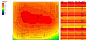
Thermal analysis of PCB
Once the Power Integrity analysis is performed we can simulate the thermal behavior of PCB itself accounting for temperature rise of PCB from each chip itself and each power plane trace itself as well. This will identify a hot spots on PCB quantified in degree Celsius (Farenheit)
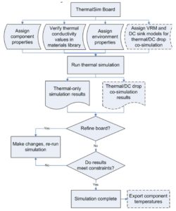
The flowchart describes the process of Thermal simulations:
Example of temperature screenshot: